- 您现在的位置:买卖IC网 > Sheet目录3882 > PIC18F4539-I/ML (Microchip Technology)IC MCU FLASH 12KX16 EE A/D 44QFN
2002 Microchip Technology Inc.
Preliminary
DS30485A-page 191
PIC18FXX39
19.1
Control Register
The Low Voltage Detect Control register controls the
operation of the Low Voltage Detect circuitry.
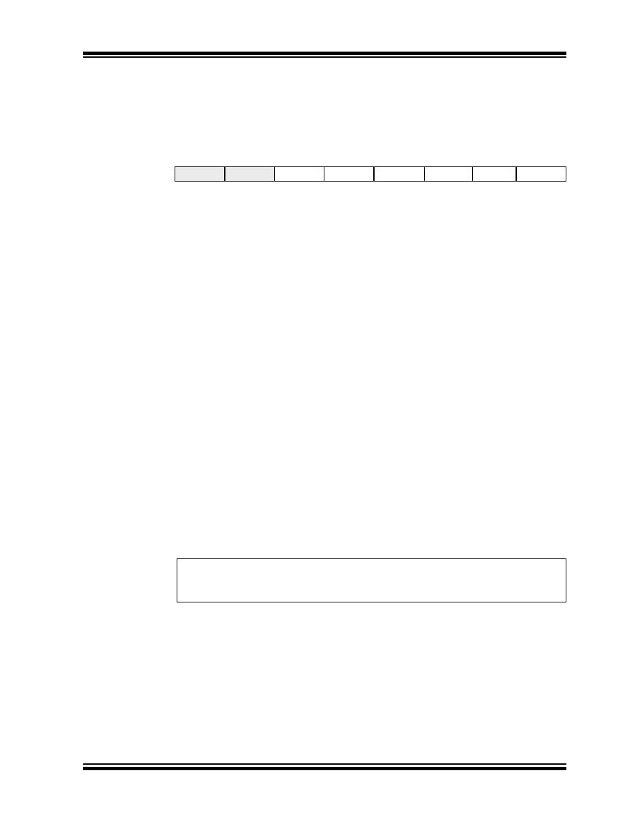
REGISTER 19-1:
LVDCON REGISTER
U-0
R-0
R/W-0
R/W-1
R/W-0
R/W-1
—
IRVST
LVDEN
LVDL3
LVDL2
LVDL1
LVDL0
bit 7
bit 0
bit 7-6
Unimplemented: Read as '0'
bit 5
IRVST: Internal Reference Voltage Stable Flag bit
1
= Indicates that the Low Voltage Detect logic will generate the interrupt flag at the
specified voltage range
0
= Indicates that the Low Voltage Detect logic will not generate the interrupt flag at the
specified voltage range and the LVD interrupt should not be enabled
bit 4
LVDEN: Low Voltage Detect Power Enable bit
1
= Enables LVD, powers up LVD circuit
0
= Disables LVD, powers down LVD circuit
bit 3-0
LVDL3:LVDL0: Low Voltage Detection Limit bits
1111
= External analog input is used (input comes from the LVDIN pin)
1110
= 4.5V - 4.77V
1101
= 4.2V - 4.45V
1100
= 4.0V - 4.24V
1011
= 3.8V - 4.03V
1010
= 3.6V - 3.82V
1001
= 3.5V - 3.71V
1000
= 3.3V - 3.50V
0111
= 3.0V - 3.18V
0110
= 2.8V - 2.97V
0101
= 2.7V - 2.86V
0100
= 2.5V - 2.65V
0011
= 2.4V - 2.54V
0010
= 2.2V - 2.33V
0001
= 2.0V - 2.12V
0000
= Reserved
Note:
LVDL3:LVDL0 modes, which result in a trip point below the valid operating voltage
of the device, are not tested.
Legend:
R = Readable bit
W = Writable bit
U = Unimplemented bit, read as ‘0’
- n = Value at POR
‘1’ = Bit is set
‘0’ = Bit is cleared
x = Bit is unknown
发布紧急采购,3分钟左右您将得到回复。
相关PDF资料
PIC18F4439-I/ML
IC MCU FLASH 6KX16 EE A/D 44QFN
PIC18F2439-I/SO
IC MCU FLASH 6KX16 EE A/D 28SOIC
PIC16F687-I/SO
IC PIC MCU FLASH 2KX14 20SOIC
PIC16F877AT-I/PTG
IC MCU FLASH 8KX14 W/AD 44 TQFP
PIC16F877A-I/LG
IC MCU FLASH 8KX14 W/AD 44PLCC
PIC12LC509AT-04I/MF
IC MCU OTP 1KX12 LV 8-DFN
PIC12C509AT-04I/MF
IC MCU OTP 1KX12 8-DFN
PIC24F08KL301-I/SS
IC MCU 16BIT 8KB FLASH 20-SSOP
相关代理商/技术参数
PIC18F4539-I/P
功能描述:8位微控制器 -MCU 24KB 1408 RAM 32 I/O RoHS:否 制造商:Silicon Labs 核心:8051 处理器系列:C8051F39x 数据总线宽度:8 bit 最大时钟频率:50 MHz 程序存储器大小:16 KB 数据 RAM 大小:1 KB 片上 ADC:Yes 工作电源电压:1.8 V to 3.6 V 工作温度范围:- 40 C to + 105 C 封装 / 箱体:QFN-20 安装风格:SMD/SMT
PIC18F4539-I/P
制造商:Microchip Technology Inc 功能描述:IC 8BIT FLASH MCU 18F4539 DIP40
PIC18F4539-I/PT
功能描述:8位微控制器 -MCU 24KB 1408 RAM 32 I/O RoHS:否 制造商:Silicon Labs 核心:8051 处理器系列:C8051F39x 数据总线宽度:8 bit 最大时钟频率:50 MHz 程序存储器大小:16 KB 数据 RAM 大小:1 KB 片上 ADC:Yes 工作电源电压:1.8 V to 3.6 V 工作温度范围:- 40 C to + 105 C 封装 / 箱体:QFN-20 安装风格:SMD/SMT
PIC18F4539IPT
制造商:MICRO CHIP 功能描述:NEW
PIC18F4539T-E/ML
功能描述:8位微控制器 -MCU 24KB 1408 RAM 32 I/O RoHS:否 制造商:Silicon Labs 核心:8051 处理器系列:C8051F39x 数据总线宽度:8 bit 最大时钟频率:50 MHz 程序存储器大小:16 KB 数据 RAM 大小:1 KB 片上 ADC:Yes 工作电源电压:1.8 V to 3.6 V 工作温度范围:- 40 C to + 105 C 封装 / 箱体:QFN-20 安装风格:SMD/SMT
PIC18F4539T-E/PT
功能描述:8位微控制器 -MCU 24KB 1408 RAM 32 I/O RoHS:否 制造商:Silicon Labs 核心:8051 处理器系列:C8051F39x 数据总线宽度:8 bit 最大时钟频率:50 MHz 程序存储器大小:16 KB 数据 RAM 大小:1 KB 片上 ADC:Yes 工作电源电压:1.8 V to 3.6 V 工作温度范围:- 40 C to + 105 C 封装 / 箱体:QFN-20 安装风格:SMD/SMT
PIC18F4539T-I/ML
功能描述:8位微控制器 -MCU 24KB 1408 RAM 32 I/O RoHS:否 制造商:Silicon Labs 核心:8051 处理器系列:C8051F39x 数据总线宽度:8 bit 最大时钟频率:50 MHz 程序存储器大小:16 KB 数据 RAM 大小:1 KB 片上 ADC:Yes 工作电源电压:1.8 V to 3.6 V 工作温度范围:- 40 C to + 105 C 封装 / 箱体:QFN-20 安装风格:SMD/SMT
PIC18F4539T-I/PT
功能描述:8位微控制器 -MCU 24KB 1408 RAM 32 I/O RoHS:否 制造商:Silicon Labs 核心:8051 处理器系列:C8051F39x 数据总线宽度:8 bit 最大时钟频率:50 MHz 程序存储器大小:16 KB 数据 RAM 大小:1 KB 片上 ADC:Yes 工作电源电压:1.8 V to 3.6 V 工作温度范围:- 40 C to + 105 C 封装 / 箱体:QFN-20 安装风格:SMD/SMT